- 您现在的位置:买卖IC网 > Sheet目录3861 > PIC18F26K80-I/MM (Microchip Technology)MCU PIC 64KB FLASH 28QFN
PIC18F66K80 FAMILY
DS39977F-page 234
2010-2012 Microchip Technology Inc.
17.2
Timer4 Interrupt
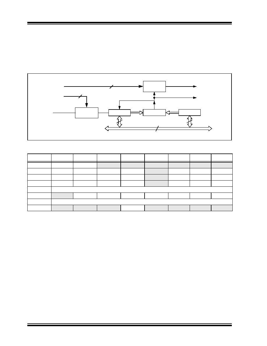
The Timer4 module has an eight-bit Period register,
PR4, that is both readable and writable. Timer4 incre-
ment from 00h until it matches PR4 and then resets to
00h on the next increment cycle. The PR4 register is
initialized to FFh upon Reset.
17.3
Output of TMR4
The outputs of TMR4 (before the postscaler) are used
only as a PWM time base for the ECCP modules. They
are not used as baud rate clocks for the MSSP module
as is the Timer2 output.
FIGURE 17-1:
TIMER4 BLOCK DIAGRAM
TABLE 17-1:
REGISTERS ASSOCIATED WITH TIMER4 AS A TIMER/COUNTER
Name
Bit 7
Bit 6
Bit 5
Bit 4
Bit 3
Bit 2
Bit 1
Bit 0
INTCON
GIE/GIEH
PEIE/GIEL
TMR0IE
INT0IE
RBIE
TMR0IF
INT0IF
RBIF
IPR4
TMR4IP
EEIP
CMP2IP
CMP1IP
—
CCP5IP
CCP4IP
CCP3IP
PIR4
TMR4IF
EEIF
CMP2IF
CMP1IF
—
CCP5IF
CCP4IF
CCP3IF
PIE4
TMR4IE
EEIE
CMP2IE
CMP1IE
—
CCP5IE
CCP4IE
CCP3IE
TMR4
Timer4 Register
T4CON
—
T4OUTPS3 T4OUTPS2 T4OUTPS1 T4OUTPS0 TMR4ON
T4CKPS1 T4CKPS0
PR4
Timer4 Period Register
PMD1
PSPMD
CTMUMD
ADCMD
TMR4MD
TMR3MD
TMR2MD
TMR1MD
TMR0MD
Legend:
— = unimplemented, read as ‘0’. Shaded cells are not used by the Timer4 module.
Comparator
TMR4 Output
TMR4
Postscaler
Prescaler
PR4
2
FOSC/4
1:1 to 1:16
1:1, 1:4, 1:16
4
T4OUTPS<3:0>
T4CKPS<1:0>
Set TMR4IF
Internal Data Bus
8
Reset
TMRx/PRx
8
(to PWM)
Match
发布紧急采购,3分钟左右您将得到回复。
相关PDF资料
PIC16C55-RC/P
IC MCU OTP 512X12 28DIP
SFW23R-2STE1
SFW23R-2STE1-FFC/FPC CONN
PIC24FJ64GA002-E/SS
IC PIC MCU FLASH 64K 28-SSOP
PIC18LF46K22-I/ML
IC PIC MCU 64KB FLASH 44QFN
PIC18F45K80-I/ML
MCU PIC 32KB FLASH 44QFN
PIC24F32KA302-I/ML
MCU 32KB FLASH 2KB RAM 28-QFN
PIC18LF45K80-I/ML
MCU PIC ECAN 32KBFLASH 44QFN
PIC18F4221-I/PT
IC PIC MCU FLASH 2KX16 44TQFP
相关代理商/技术参数
PIC18F26K80-I/SO
功能描述:8位微控制器 -MCU 64KB FL 4KBRM 16MIPS 12bit ADC CTMU RoHS:否 制造商:Silicon Labs 核心:8051 处理器系列:C8051F39x 数据总线宽度:8 bit 最大时钟频率:50 MHz 程序存储器大小:16 KB 数据 RAM 大小:1 KB 片上 ADC:Yes 工作电源电压:1.8 V to 3.6 V 工作温度范围:- 40 C to + 105 C 封装 / 箱体:QFN-20 安装风格:SMD/SMT
PIC18F26K80-I/SP
功能描述:8位微控制器 -MCU 64KB FL 4KBRM 16MIPS 12bit ADC CTMU RoHS:否 制造商:Silicon Labs 核心:8051 处理器系列:C8051F39x 数据总线宽度:8 bit 最大时钟频率:50 MHz 程序存储器大小:16 KB 数据 RAM 大小:1 KB 片上 ADC:Yes 工作电源电压:1.8 V to 3.6 V 工作温度范围:- 40 C to + 105 C 封装 / 箱体:QFN-20 安装风格:SMD/SMT
PIC18F26K80-I/SS
功能描述:8位微控制器 -MCU 64KB FL 4KBRM 16MIPS 12bit ADC CTMU RoHS:否 制造商:Silicon Labs 核心:8051 处理器系列:C8051F39x 数据总线宽度:8 bit 最大时钟频率:50 MHz 程序存储器大小:16 KB 数据 RAM 大小:1 KB 片上 ADC:Yes 工作电源电压:1.8 V to 3.6 V 工作温度范围:- 40 C to + 105 C 封装 / 箱体:QFN-20 安装风格:SMD/SMT
PIC18F26K80T-I/ML
功能描述:8位微控制器 -MCU 64KB FL 4KBRM 16MIPS 12bit ADC CTMU RoHS:否 制造商:Silicon Labs 核心:8051 处理器系列:C8051F39x 数据总线宽度:8 bit 最大时钟频率:50 MHz 程序存储器大小:16 KB 数据 RAM 大小:1 KB 片上 ADC:Yes 工作电源电压:1.8 V to 3.6 V 工作温度范围:- 40 C to + 105 C 封装 / 箱体:QFN-20 安装风格:SMD/SMT
PIC18F26K80T-I/MM
功能描述:8位微控制器 -MCU ECAN 64KB FL 4KBRM 16 MIPS 12b ADC CTMU RoHS:否 制造商:Silicon Labs 核心:8051 处理器系列:C8051F39x 数据总线宽度:8 bit 最大时钟频率:50 MHz 程序存储器大小:16 KB 数据 RAM 大小:1 KB 片上 ADC:Yes 工作电源电压:1.8 V to 3.6 V 工作温度范围:- 40 C to + 105 C 封装 / 箱体:QFN-20 安装风格:SMD/SMT
PIC18F26K80T-I/SO
功能描述:8位微控制器 -MCU 64KB FL 4KBRM 16MIPS 12bit ADC CTMU RoHS:否 制造商:Silicon Labs 核心:8051 处理器系列:C8051F39x 数据总线宽度:8 bit 最大时钟频率:50 MHz 程序存储器大小:16 KB 数据 RAM 大小:1 KB 片上 ADC:Yes 工作电源电压:1.8 V to 3.6 V 工作温度范围:- 40 C to + 105 C 封装 / 箱体:QFN-20 安装风格:SMD/SMT
PIC18F26K80T-I/SS
功能描述:8位微控制器 -MCU 64KB FL 4KBRM 16MIPS 12bit ADC CTMU RoHS:否 制造商:Silicon Labs 核心:8051 处理器系列:C8051F39x 数据总线宽度:8 bit 最大时钟频率:50 MHz 程序存储器大小:16 KB 数据 RAM 大小:1 KB 片上 ADC:Yes 工作电源电压:1.8 V to 3.6 V 工作温度范围:- 40 C to + 105 C 封装 / 箱体:QFN-20 安装风格:SMD/SMT
PIC18F27J13-I/ML
功能描述:8位微控制器 -MCU 128KB Flash 4KB RAM 12MIPS nanoWatt RoHS:否 制造商:Silicon Labs 核心:8051 处理器系列:C8051F39x 数据总线宽度:8 bit 最大时钟频率:50 MHz 程序存储器大小:16 KB 数据 RAM 大小:1 KB 片上 ADC:Yes 工作电源电压:1.8 V to 3.6 V 工作温度范围:- 40 C to + 105 C 封装 / 箱体:QFN-20 安装风格:SMD/SMT